Authors: Fengdeng Liu, Zhifei Yang, David Abramovitch, Silu Guo, K. Andre Mkhoyan, Marco Bernardi, Bharat Jalan
Published on: May 14, 2024
Impact Score: 7.2
Arxiv code: Arxiv:2405.08915
Summary
- What is new: The paper presents a novel approach to achieve both high transparency and high conductivity in ultra-wide bandgap (UWBG) semiconductors using a thin heterostructure design.
- Why this is important: Finding a semiconductor that maintains high transparency to DUV wavelengths while being highly conductive with good mobility at room temperature.
- What the research proposes: Using a heterostructure of SrSnO3/La:SrSnO3/GdScO3 (110) with electrostatic gating to manage carrier density and mobility, ensuring transparency and conductivity.
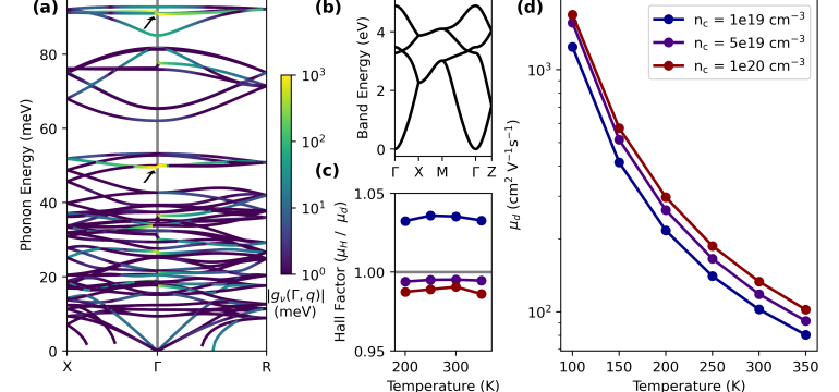
- Results: Achieved a carrier density modulation from 1018 cm-3 to 1020 cm-3, room temperature mobility from 40 to 140 cm2V-1s-1, and 85% optical transparency at a 300 nm wavelength.
Technical Details
Technological frameworks used: nan
Models used: First principles calculations for phonon-limited mobility, experimental setup for testing transparency and conductivity.
Data used: Carrier density, mobility measurements, optical transparency data
Potential Impact
Markets in high-power electronics and deep-ultraviolet optoelectronics, potentially impacting companies developing UV sterilization tools and high-power electronic devices.
Want to implement this idea in a business?
We have generated a startup concept here: ClearPowerTech.


Leave a Reply