Authors: Wenyu Song, Zehao Yu, Yuhao Wang, Yichun Gao, Zonglin Li, Shuai Yang, Shan Zhang, Zuhan Geng, Ruidong Li, Zhaoyu Wang, Fangting Chen, Lining Yang, Wentao Miao, Jiaye Xu, Xiao Feng, Tiantian Wang, Yunyi Zang, Lin Li, Runan Shang, Qi-Kun Xue, Ke He, Hao Zhang
Published on: February 03, 2024
Impact Score: 8.22
Arxiv code: Arxiv:2402.02132
Summary
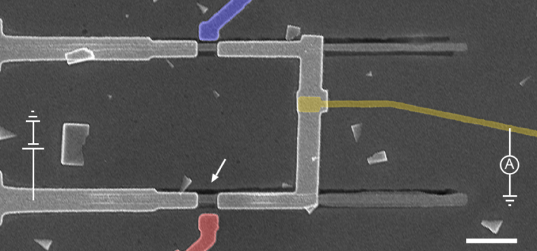
- What is new: Embedding PbTe nanowires within a lattice-matched crystal to tackle surface disorder, using self-organized growth for nearly-atomic-flat edges, and achieving quantized conductance plateaus without a magnetic field over channel lengths of 1.54 $\mu$m.
- Why this is important: Surface disorder in Majorana nanowires constrains device performance, making it difficult to observe Majoranas definitively.
- What the research proposes: Using a novel growth method to embed PbTe nanowires within a crystal that matches its lattice, avoiding oxide and creating nearly-perfect flat wire edges, coupled with Pb film for a flat interface and large superconducting gap.
- Results: Significantly improved channel lengths and superconducting gap, with quantized conductance plateaus observed at zero magnetic field, indicating a major step towards the observation of Majoranas.
Technical Details
Technological frameworks used: Self-organized growth for nanowire embedding and shaping
Models used: Lattice-matched crystal embedding, coupled with Pb film for superconducting interface
Data used: Observations of quantized conductance and superconducting gap measurements
Potential Impact
Semiconductor industry, quantum computing companies, materials science research firms
Want to implement this idea in a business?
We have generated a startup concept here: QuantumFlow.


Leave a Reply